Industrial experts in MEMS/NEMS, Production oriented FEA based design, Process integration, Optimized Mask layout, Qualification, Production Transfer, Failure analysis, 3D Modelling, FEA based Packaging Analysis.
From process development to high-volume manufacturing transfer — precision engineering at every scale, from wafer to device.
FEA based micro/nano structure design following Design for Six Sigma methodology. Optimum mask layout for stepper, contact and direct write. Solid modelling for packaging and packaging analysis.
End-to-end MEMS process flow design, multi-mask process development, and optimization for yield and device performance.
Process setup including equipment procurement, process and equipment qualification, and comprehensive standard operating procedure documentation.
Proven track record transferring R&D processes to high-volume manufacturing partners. Process qualification, yield optimization, and full documentation for seamless production scale-up.
SBIR/STTR proposal writing, process documentation, patent preparation support, and peer-review quality technical reporting.
Technical advisory for investors and startups, equipment evaluation, vendor selection, and process feasibility assessment.
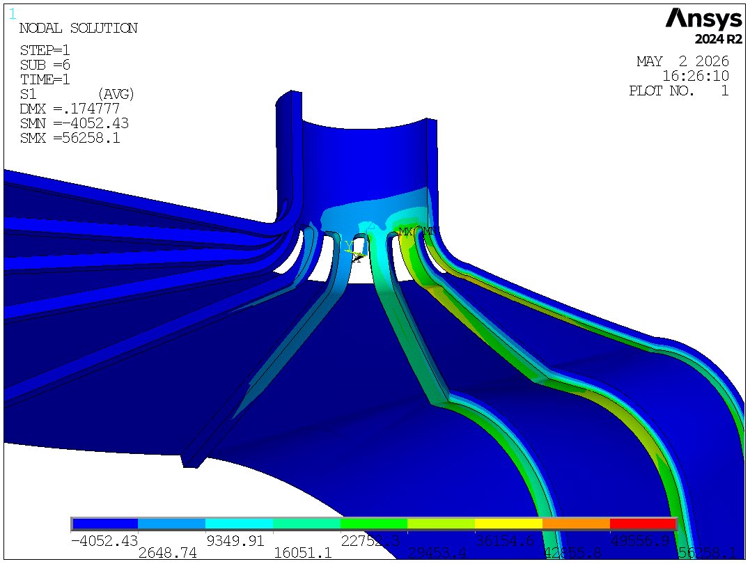
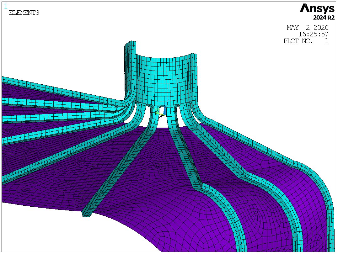
Every design at SF NEMS & MEMS undergoes rigorous FEA simulation up front to improve device reliability and minimize failure rate before any material is touched. Structural, modal, and stress analysis performed in ANSYS to validate geometry, identify stress concentration zones, and in the project shown to the right, optimize suspension spring designs for maximum yield and performance.
ANSYS 2024 R2 · Nodal Solution S1 · SMX = 56,258 psi
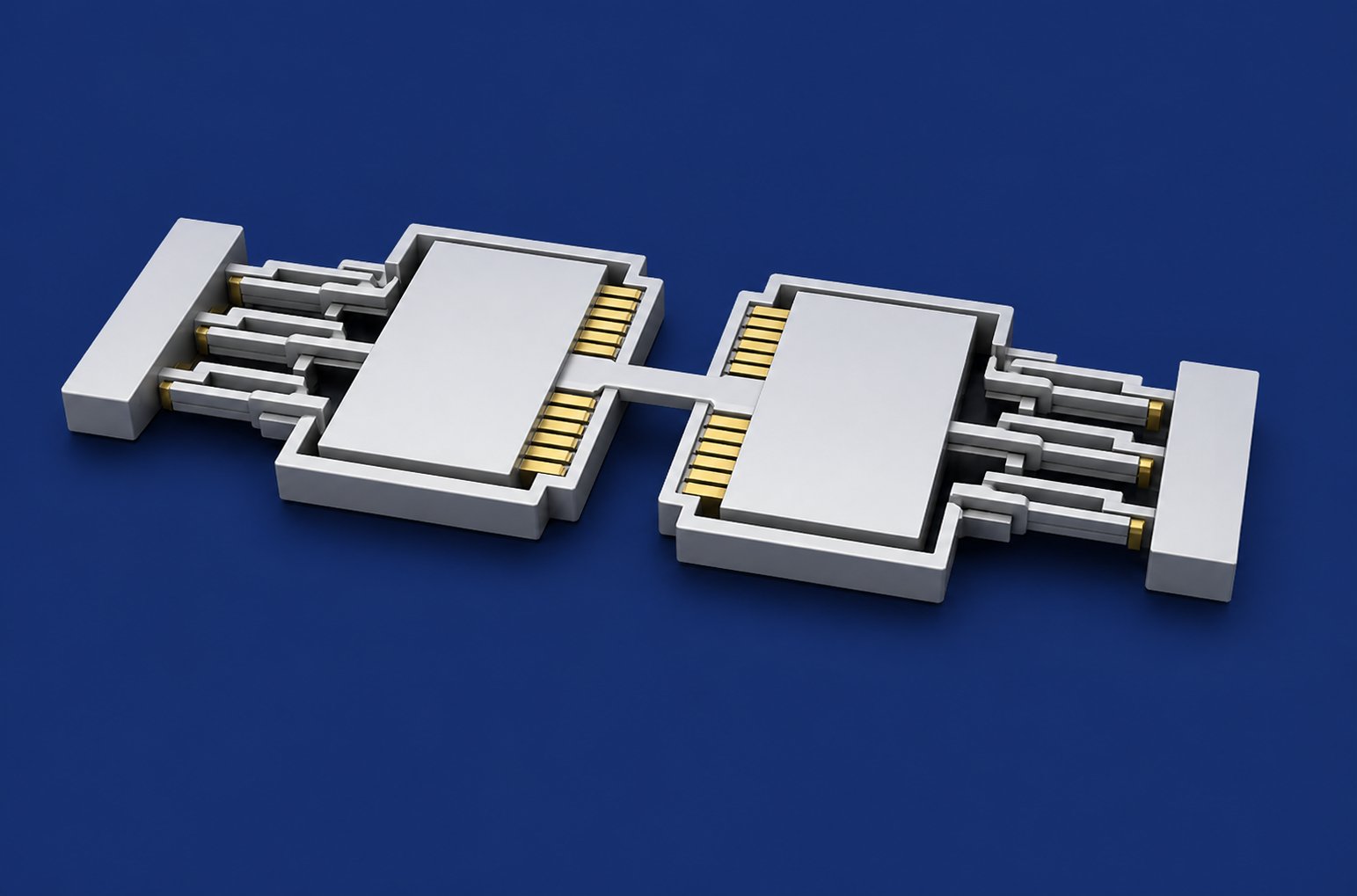
High-performance silicon MEMS tuning fork gyroscope featuring two symmetrical proof masses connected via a central coupling beam. Interdigitated gold comb drive electrodes on lateral sides enable anti-phase drive mode actuation. Folded suspension springs provide mechanical compliance in drive axis while maintaining sense-axis stiffness. Designed for mode-matched operation with high-Q resonance and ultra-low noise angular rate detection.
* Image for demonstration purpose only.
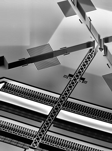
Silicon MEMS optical switch featuring electrostatic comb drive actuators, folded beam suspension springs, and precision-etched mirror structures. Developed for low-loss optical path switching with high repeatability and fast response time.
* Image for demonstration purpose only.
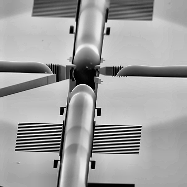
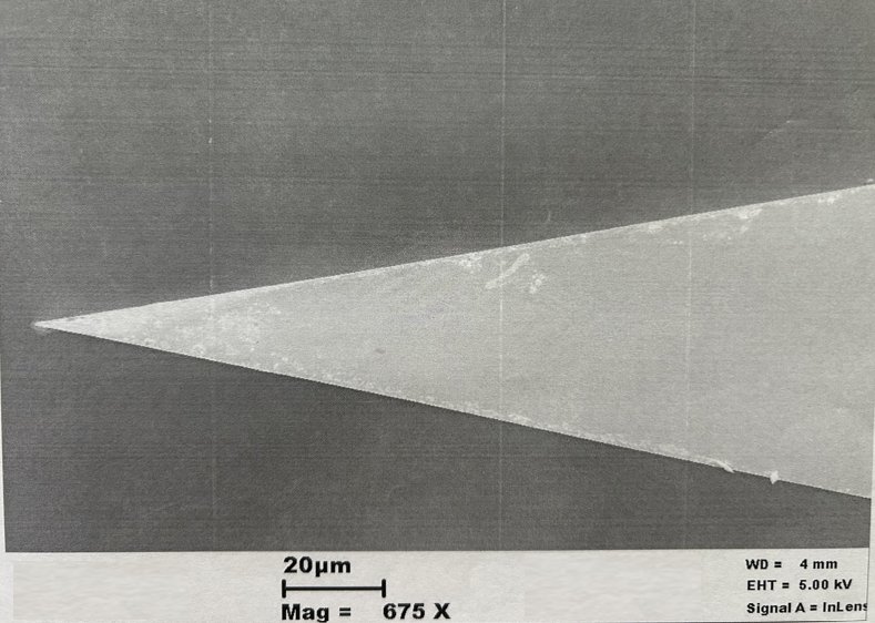
Microfabricated silicon microneedle arrays for transdermal drug delivery applications. Sharp needle tips with sub-micron apex radius achieved through optimized proprietary etch process. SEM image shows needle tip at 675× magnification — 20μm scale bar confirms precision geometry.
SF NEMS & MEMS delivers expert MEMS/NEMS design, FEA-driven multiphysics modeling, process development, and microfabrication solutions for semiconductor companies, startups, and research institutions.
Our industry-proven team brings decades-long expertise in both FEA-based design and hands-on fabrication, developed across advanced environments including GE, Merit Medical, HP, and premier research facilities such as the Stanford Nanofabrication Facility.
We integrate physics-based simulation with deep process knowledge to ensure designs are not only innovative, but fabrication-ready and performance-optimized.
From concept through production, we bridge the critical gap between R&D and manufacturing — translating complex designs into robust, scalable, and yield-driven processes.
Whether you need process development support, cleanroom guidance, or technical consulting — we're ready to engage. Initial consultations are available remotely or in-person in the Bay Area.
SF NEMS & MEMS periodically makes surplus wafers available for direct purchase. These are high-quality materials sourced from completed projects. Inventory changes frequently — we encourage you to check back regularly or contact us to be notified when new stock becomes available.